- 您现在的位置:买卖IC网 > Sheet目录3881 > PIC18F4539T-E/ML (Microchip Technology)IC PIC MCU FLASH 12KX16 44QFN
PIC18F2682/2685/4682/4685
DS39761C-page 308
2009 Microchip Technology Inc.
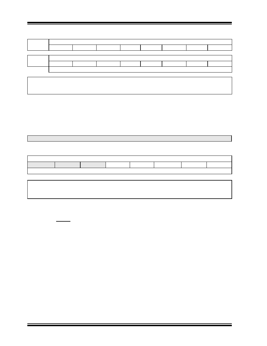
REGISTER 23-45: RXFCONn: RECEIVE FILTER CONTROL REGISTER n [0
≤ n ≤ 1](1)
RXFCON0
R/W-0
R/W-1
RXF7EN
RXF6EN
RXF5EN
RXF4EN
RXF3EN
RXF2EN
RXF1EN
RXF0EN
RXFCON1
R/W-0
R/W-1
R/W-0
RXF15EN
RXF14EN
RXF13EN
RXF12EN RXF11EN
RXF10EN
RXF9EN
RXF8EN
bit 7
bit 0
Legend:
C = Clearable bit
R = Readable bit
W = Writable bit
U = Unimplemented bit, read as ‘0’
-n = Value at POR
‘1’ = Bit is set
‘0’ = Bit is cleared
x = Bit is unknown
bit 7-0
RXFnEN: Receive Filter n Enable bits
0 = Filter is disabled
1 = Filter is enabled
Note 1:
This register is available in Mode 1 and 2 only.
Note:
Register 23-46 through Register 23-51 are writable in Configuration mode only.
REGISTER 23-46: SDFLC: STANDARD DATA BYTES FILTER LENGTH COUNT REGISTER(1)
U-0
R/W-0
—
FLC4
FLC3
FLC2
FLC1
FLC0
bit 7
bit 0
Legend:
R = Readable bit
W = Writable bit
U = Unimplemented bit, read as ‘0’
-n = Value at POR
‘1’ = Bit is set
‘0’ = Bit is cleared
x = Bit is unknown
bit 7-5
Unimplemented: Read as ‘0’
bit 4-0
FLC4:FLC0: Filter Length Count bits
Mode 0:
Not used; forced to ‘00000’.
00000-10010 = 0
18 bits are available for standard data byte filter. Actual number of bits used
depends on DLC3:DLC0 bits (RXBnDLC<3:0> or BnDLC<3:0> if configured
as RX buffer) of message being received.
If DLC3:DLC0 = 0000 No bits will be compared with incoming data bits.
If DLC3:DLC0 = 0001 Up to 8 data bits of RXFnEID<7:0>, as determined by FLC2:FLC0, will be
compared with the corresponding number of data bits of the incoming
message.
If DLC3:DLC0 = 0010 Up to 16 data bits of RXFnEID<15:0>, as determined by FLC3:FLC0, will be
compared with the corresponding number of data bits of the incoming
message.
If DLC3:DLC0 = 0011 Up to 18 data bits of RXFnEID<17:0>, as determined by FLC4:FLC0, will be
compared with the corresponding number of data bits of the incoming
message.
Note 1:
This register is available in Mode 1 and 2 only.
发布紧急采购,3分钟左右您将得到回复。
相关PDF资料
PIC18LF8680T-I/PT
IC PIC MCU FLASH 32KX16 80TQFP
PIC16F1936-I/SO
IC PIC MCU FLASH 512KX14 28-SOIC
PIC18F24K20-I/SO
IC PIC MCU FLASH 8KX16 28SOIC
PIC18LF8585T-I/PT
IC PIC MCU FLASH 24KX16 80TQFP
XF2J-3024-11
CONN FPC 30POS 0.5MM SMT
PIC18LF6525T-I/PT
IC PIC MCU FLASH 24KX16 64TQFP
PIC18LF8621T-I/PT
IC PIC MCU FLASH 32KX16 80TQFP
PIC18F8620T-E/PT
IC PIC MCU FLASH 32KX16 80TQFP
相关代理商/技术参数
PIC18F4539T-E/PT
功能描述:8位微控制器 -MCU 24KB 1408 RAM 32 I/O RoHS:否 制造商:Silicon Labs 核心:8051 处理器系列:C8051F39x 数据总线宽度:8 bit 最大时钟频率:50 MHz 程序存储器大小:16 KB 数据 RAM 大小:1 KB 片上 ADC:Yes 工作电源电压:1.8 V to 3.6 V 工作温度范围:- 40 C to + 105 C 封装 / 箱体:QFN-20 安装风格:SMD/SMT
PIC18F4539T-I/ML
功能描述:8位微控制器 -MCU 24KB 1408 RAM 32 I/O RoHS:否 制造商:Silicon Labs 核心:8051 处理器系列:C8051F39x 数据总线宽度:8 bit 最大时钟频率:50 MHz 程序存储器大小:16 KB 数据 RAM 大小:1 KB 片上 ADC:Yes 工作电源电压:1.8 V to 3.6 V 工作温度范围:- 40 C to + 105 C 封装 / 箱体:QFN-20 安装风格:SMD/SMT
PIC18F4539T-I/PT
功能描述:8位微控制器 -MCU 24KB 1408 RAM 32 I/O RoHS:否 制造商:Silicon Labs 核心:8051 处理器系列:C8051F39x 数据总线宽度:8 bit 最大时钟频率:50 MHz 程序存储器大小:16 KB 数据 RAM 大小:1 KB 片上 ADC:Yes 工作电源电压:1.8 V to 3.6 V 工作温度范围:- 40 C to + 105 C 封装 / 箱体:QFN-20 安装风格:SMD/SMT
PIC18F4550EPT
制造商:Microchip Technology Inc 功能描述:
PIC18F4550-I/ML
功能描述:8位微控制器 -MCU 32kBF 2048RM FSUSB2 RoHS:否 制造商:Silicon Labs 核心:8051 处理器系列:C8051F39x 数据总线宽度:8 bit 最大时钟频率:50 MHz 程序存储器大小:16 KB 数据 RAM 大小:1 KB 片上 ADC:Yes 工作电源电压:1.8 V to 3.6 V 工作温度范围:- 40 C to + 105 C 封装 / 箱体:QFN-20 安装风格:SMD/SMT
PIC18F4550-I/P
功能描述:8位微控制器 -MCU 32kBF 2048RM FSUSB2 RoHS:否 制造商:Silicon Labs 核心:8051 处理器系列:C8051F39x 数据总线宽度:8 bit 最大时钟频率:50 MHz 程序存储器大小:16 KB 数据 RAM 大小:1 KB 片上 ADC:Yes 工作电源电压:1.8 V to 3.6 V 工作温度范围:- 40 C to + 105 C 封装 / 箱体:QFN-20 安装风格:SMD/SMT
PIC18F4550-I/PT
功能描述:8位微控制器 -MCU 32kBF 2048RM FSUSB2 RoHS:否 制造商:Silicon Labs 核心:8051 处理器系列:C8051F39x 数据总线宽度:8 bit 最大时钟频率:50 MHz 程序存储器大小:16 KB 数据 RAM 大小:1 KB 片上 ADC:Yes 工作电源电压:1.8 V to 3.6 V 工作温度范围:- 40 C to + 105 C 封装 / 箱体:QFN-20 安装风格:SMD/SMT
PIC18F4550T-I/ML
功能描述:8位微控制器 -MCU 32kBF 2048RM FSUSB2 RoHS:否 制造商:Silicon Labs 核心:8051 处理器系列:C8051F39x 数据总线宽度:8 bit 最大时钟频率:50 MHz 程序存储器大小:16 KB 数据 RAM 大小:1 KB 片上 ADC:Yes 工作电源电压:1.8 V to 3.6 V 工作温度范围:- 40 C to + 105 C 封装 / 箱体:QFN-20 安装风格:SMD/SMT